StephensDev
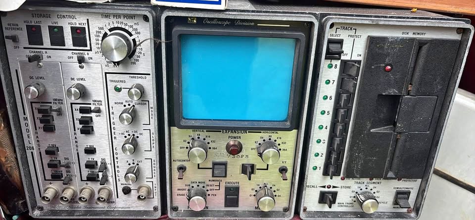
Nicolet 2090 III Oscilloscope
Contents
- Nicolet 2090 III Oscilloscope
- Acquisition
- Initial Inspection
- Troubleshooting
- Power Supply Diagnosis
- Initial Repairs
- Round 2
- III BAY POWER SUPPLY - Connection Chart
- Transformer Windings & AC Input
- Rectifiers and Capacitors
- Voltage Regulators & Transistors
- Output Connections
- MOVs (Transient Voltage Suppression)
- Important Resistors / Trimmers
- Summary Flow
- References
Acquisition
Acquired in June 2025 as my first oscilloscope for $60.
Initial Inspection
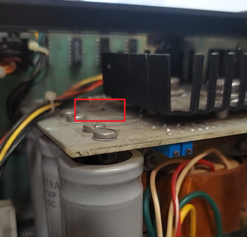
I removed the side panels to inspect the internals. Aside from being a bit dusty, nothing looked obviously wrong. However, when I attempted to power it on, nothing happened.
I checked the fuse — a 60×30mm 3A glass fuse — and confirmed it was blown. After replacing it, the oscilloscope emitted a considerable amount of smoke from the floppy drive section.
Opening it back up, I discovered burn marks on the power supply board labeled:
Nicolet Instrument
Corp Power Supply
Floppy Disk 6-20-78
000-9021-03
The oscilloscope is divided into three main sections:
- Oscilloscope (Model 206)
- CRT and control board
- Floppy drive subsystem
Troubleshooting
To isolate the problem, I disconnected the floppy section and was able to successfully power on the oscilloscope. This suggests that the core oscilloscope is still functional, but the floppy system and its power supply are faulty. That means I likely won't be able to use the I/O power or floppy save features, but the oscilloscope itself can still function independently.
That said, I decided to try repairing the floppy power supply.
Power Supply Diagnosis
The floppy subsystem has its own power supply that converts AC into:
- +5V DC
- +12V DC
- –5V DC
These are used by the CPU board, the floppy drive, and the floppy controller.
In a worst-case scenario, I could replace the damaged power board with a 12V dc wall adapter and a PicoPSU to generate the necessary voltages. But first, I removed the board for closer inspection.
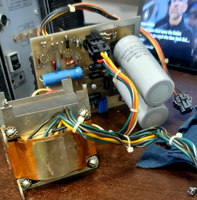
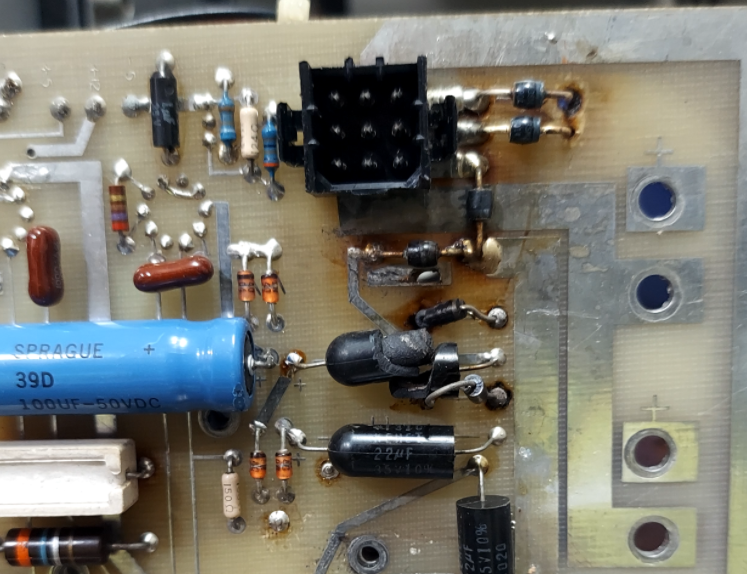
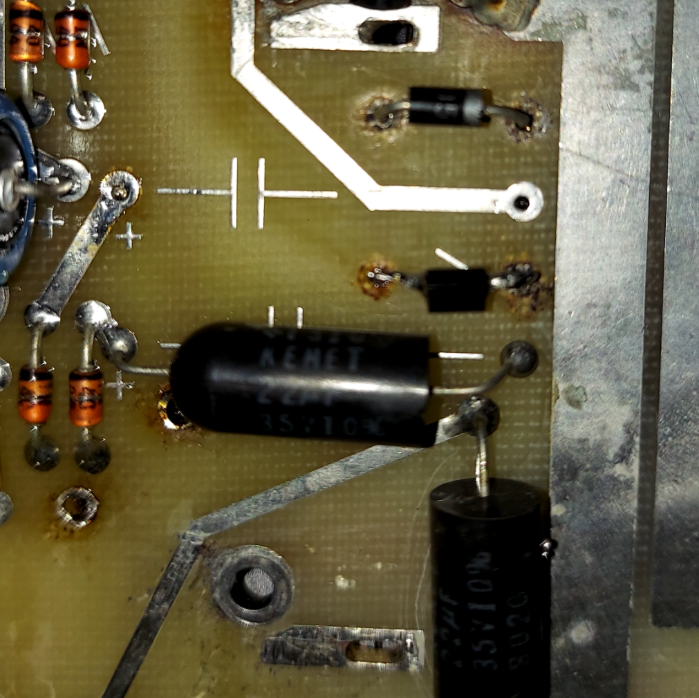
The board had visible burn marks, and one tantalum capacitor had clearly blown. After testing nearby components and checking against the schematic, I found the following failed parts:
- 1 × 22µF 35V 10% axial tantalum capacitor
- 2 × 1N4004 diodes
The damaged components were located right next to the blown capacitor.
Initial Repairs
While I wait for a replacement capacitor to arrive, I’ve started partial repairs:
- Replaced one 1N4004 diode with a 1N4005
- Replaced the second diode with an RS2M (SMD type), by soldering on leads salvaged from a resistor to adapt it for through-hole mounting
Once the new capacitor arrives, I’ll install it and attempt a full power-up of the floppy section.
Round 2
The new capacitors arrived, but I realized they were ceramic, not tantalum.
However, they were rated 22 µF 50 V 10%, exceeding the original spec, and being non-polarized meant easier installation. So I gave it a try.
Hovering my hand over the power switch, I powered it on.
A spark appeared immediately, and I shut it off. The fuse survived, but both replacement diodes failed again.
The capacitor appears unharmed on initial inspection.
III BAY POWER SUPPLY - Connection Chart
Schematic 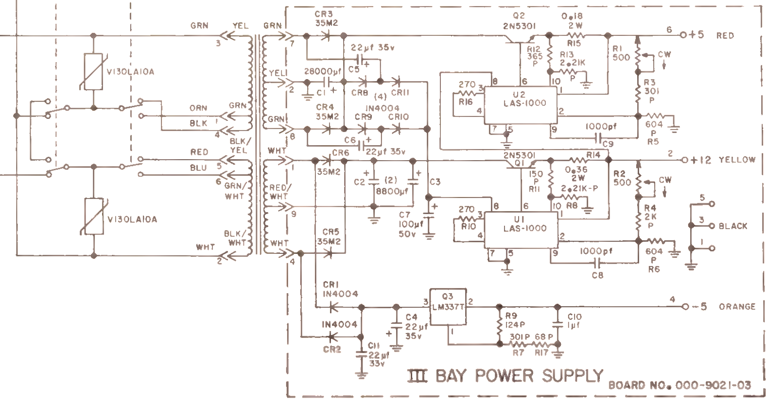
Transformer Windings & AC Input
| Pin | Wire Color | Voltage (Measured) | Function |
|---|---|---|---|
| 3 | GRN | – | AC Primary Input |
| 4 | BLK/YEL | – | AC Primary Input |
| 5 | BLU | – | AC Primary Input |
| 6 | GRN/WHT | – | AC Primary Input |
| 2 | BLK/WHT | – | Neutral / AC Return |
| 7-8 | GRN–WHT | ~15.5 VAC | Secondary winding #1 (+5V supply) |
| 9-4 | RED/WHT–WHT | ~7.5 VAC | Secondary winding #2 (±12V and –5V supply) |
Rectifiers and Capacitors
| Part | Type | Function | Connects To |
|---|---|---|---|
| CR1–CR2 | 1N4004 | –5V Bridge Rectifier | Transformer pins 9 & 4 |
| CR3–CR4 | 35M2 | +5V Bridge (part of full bridge) | Transformer pins 7 & 8 |
| CR5–CR6 | 35M2 | +12V Bridge | Transformer pins 9 & 4 |
| CR9–CR10 | 1N4004 | +5V Bridge (part of full bridge) | Transformer pins 7 & 8 |
| C1, C2 | 8800 µF | Bulk filter for +5V | After CR3–CR4–CR9–CR10 bridge |
| C5, C6 | 22 µF 35V | Secondary filter for +5V | After bridge |
| C3 | 8800 µF | Bulk filter for +12V | After CR5–CR6 |
| C7 | 100 µF 50V | Filter for +12V | After C3 |
| C4, C11 | 22 µF 35V | Filter for –5V | After CR1–CR2 |
| C10 | 1 µF | Filter at LM337 output | LM337 regulator output |
| C8, C9 | 1000 pF | Stability caps for LAS-1000 | Voltage regulators |
Voltage Regulators & Transistors
| Designator | Part | Function | Output Voltage | Notes |
|---|---|---|---|---|
| Q2 | 2N5301 | Pass transistor | +5V | Works with U2 LAS-1000 |
| U2 | LAS-1000 | Voltage regulator | +5V | Regulates output voltage |
| Q1 | 2N5301 | Pass transistor | +12V | Works with U1 LAS-1000 |
| U1 | LAS-1000 | Voltage regulator | +12V | Regulates output voltage |
| Q3 | LM337T | Negative regulator | –5V | Provides negative voltage |
Output Connections
| Pin | Color | Voltage | Description |
|---|---|---|---|
| 6 | RED | +5V | Primary logic power |
| 2 | YELLOW | +12V | Floppy motor / logic |
| 4 | ORANGE | –5V | Negative rail |
| 5 | BLACK | GND | Common ground |
| 1, 3 | Various | GND | Common ground |
MOVs (Transient Voltage Suppression)
| Designator | Part | Location | Purpose |
|---|---|---|---|
| V130LA10A | MOV | Across AC primary lines | Suppresses voltage spikes |
Important Resistors / Trimmers
| Designator | Value | Purpose |
|---|---|---|
| R1 – R6 | Various pots | Regulator feedback and tuning |
| R7 – R17 | Fixed values | LM337 regulator compensation |
Summary Flow
- AC Mains Input
- Transformer
- Rectifier Bridge (CRx)
- Bulk Capacitors (C1–C7)
- Voltage Regulators & Pass Transistors (Q1/Q2/Q3, U1/U2)
- Outputs: +5V, +12V, –5V, GND